Nio Band Gap

Optical Band Gap Of Nio Thin Films Obtained From Transmission Download Scientific Diagram
A B C Optical Band Gap Of Nickel Oxide Nio Films At Different Download Scientific Diagram

A C Uv Vis Spectra And B D Band Gap Energy Plot Of Nio Nanoparticles Download Scientific Diagram

Absorbance Curve Band Gap Of Nio A As Prepared B 350 C And C Download Scientific Diagram

Optical Energy Band Gap Of Nio From Ahn 2 Vs Hn And Plot Of The Download Scientific Diagram

Estimation Of Band Gap Energy Eg From Tauc S Relation Of Nio Thin Download Scientific Diagram

Nanosized nio is also used in alkaline batteries electrochemical capacitors smart windows and as an active layer for gas sensors.
Nio band gap. The mineralogical form of nio bunsenite is very rare other nickel iii oxides have been claimed for example. Nickel ii oxide is the chemical compound with the formula nio it is the principal oxide of nickel. Prl 102 226401 2009. Nio was chosen as the p type interfacial layer.
Convenient way to specify a basis set. Fixing the band gap of zns with the tb mbj model potential. They have been used as catalysts 4 electrochromic display devices 5 fuel cells 6 and gas sensors 7. Several million kilograms are produced annually of varying quality mainly as an intermediate in the production of nickel alloys.
The band structure of a strongly correlated semiconductor as nio has been the object of much debate prl 103 036404 2009. Our first principles quantum mechanics calculations show band gaps dramatically decrease to 2 0 ev when nio is alloyed with li 2 o. Nickel oxide nio films have a wide range of applications due to their excellent chemical sta bility. Nio is a p type semiconductor transition metal oxide which includes direct band gaps of 3 5 3 8 ev.
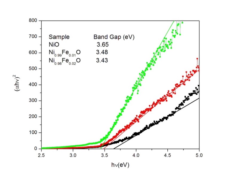
Uv visible characterization of these samples indicated that the optical band gap of nio decreased from 3 65 to 3 43 ev when the doping concentration increased from x 0 to x 0 02. Fixing the band gap of nio with gga u. This unique structure results in a range of intriguing characteristics which mean that nio nanomaterials can be successfully employed in a range of physical applications. Nanostructured nio has a wide range of applications as a p type semiconductor with a stable wide band gap 3 6 4 0 ev although bulk nio is an antiferromagnetic insulator.
Nio is a well known antiferromagnetic material 1 and a metal deficient p type semiconductor 2 with a 3 6 ev band gap 3. Tuning precision and performance. It is classified as a basic metal oxide. Dft 1 2 method for silicon.
Most authors using computational techniques well beyond the simple density functional theory and the approximations gga or lda claim that the band gap is about 4 0 ev and that the conduction band is of ni 3d nature. Although argu ably the most studied and modeled of binary transition metal oxides exact details of the band structure band gap e g fermi level e f conduction band minimum cbm valence band maximum vbm and conduction mechanism continue to stimulate discussion 39 43 45.

The Optical Band Gap Energy Of A Bare Nio Inset Uv Vis Absorption Download Scientific Diagram
Optical Band Gap Energy Absorbance And Reflectance Spectra Of Nio Download Scientific Diagram
Http Www Pnas Org Content 105 8 2783 Full Pdf With Ds Yes
Fe Doping Induced Shrinking Of Band Gap Of Nio Nanoparticles

Uv Vis Absorbance Of Nio I Nps Inset Picture Indicate The Band Gap Download Scientific Diagram

Varition Of Optical Band Gap For Pure And Nb Doped Nio Thin Films Download Scientific Diagram

A Absorbance And B Band Gap Of The Cuo Nio Zno Mixed Oxide Download Scientific Diagram
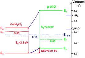
Photoelectrochemical Performance Enhanced By A Nickel Oxide Hematite P N Junction Photoanode Chemical Communications Rsc Publishing
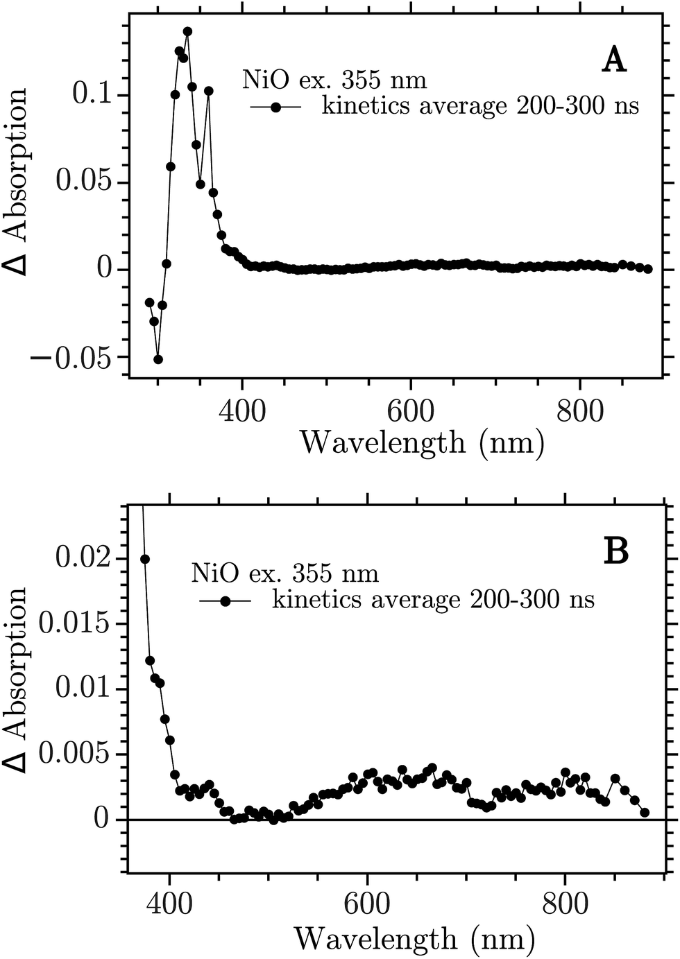
Unveiling Hole Trapping And Surface Dynamics Of Nio Nanoparticles Chemical Science Rsc Publishing Doi 10 1039 C7sc03442c

Nonmagnetic Band Structure Of Nio Obtained By The Lmto Method The Download Scientific Diagram

A Uv Vis Absorption And B Tauc S Plots For The Calculation Of Band Download Scientific Diagram
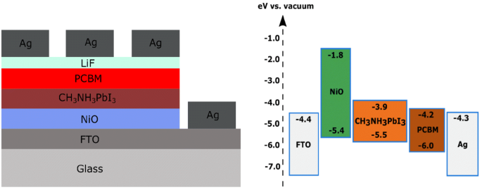
Thermal Oxidation Of Sputtered Nickel Nano Film As Hole Transport Layer For High Performance Perovskite Solar Cells Springerlink

Band Gap Of Nio Cr And Co Doped Nio Nanoparticles Download Table
